NESS ENGINEERING
SOLID STATE MODULATOR EXPERIENCE


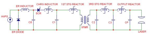
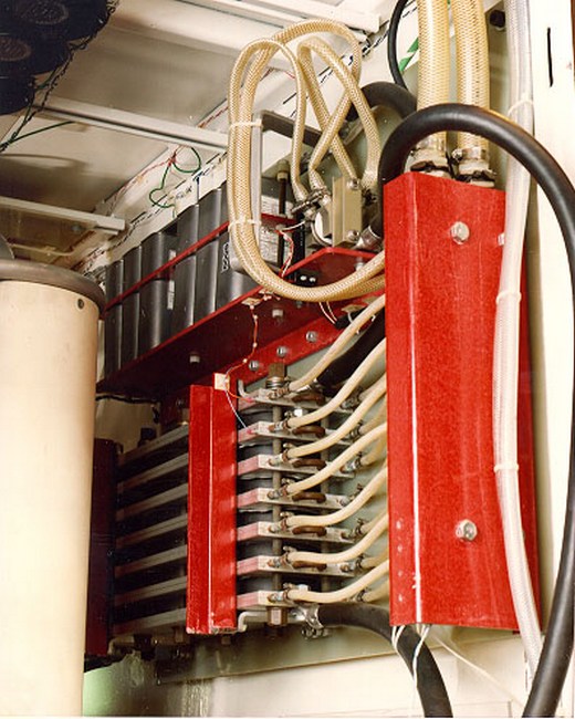
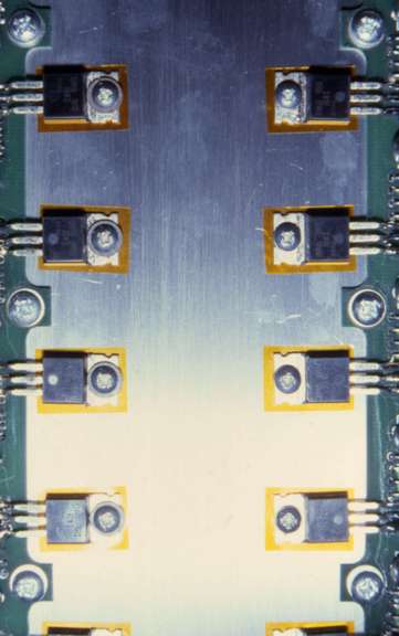
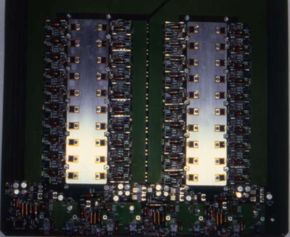
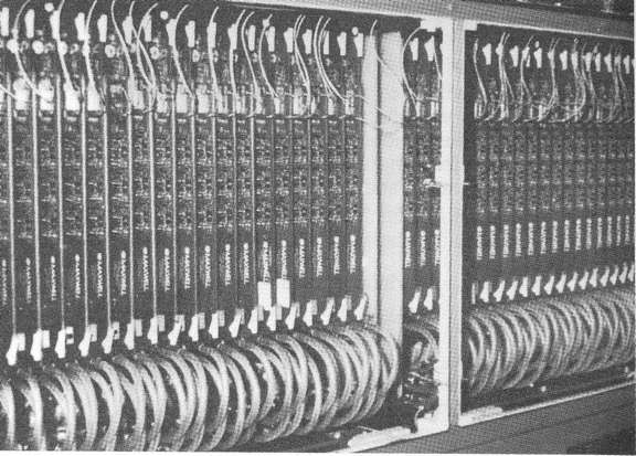
Solid state modulators are typically developed for driving pulsed high voltage loads. The biggest advantage of solid state switching is that the switching devices can have a virtually unlimited lifetime. While other high power switches, such as thyratrons and spark gaps, have characteristics that limit the lifetime to some finite level (typically the heater/reservoir life for thyratrons and electrode erosion or insulator coating for spark gaps), solid state devices don't have similar equivalent limiters (wire bond fatigue can limit lifetime in some cases but with suitable device de-rating, even that can be managed to still provide very long lifetimes). As a result, the maintenance costs of such a system can be lower than that of a design using other switch devices. Unfortunately, the peak power handling capability of solid state devices is usually not as high as that obtainable from other switches. As a result, series and/or parallel arrays of devices are often required to meet the overall switching requirements.

Solid State Switching Technologies:
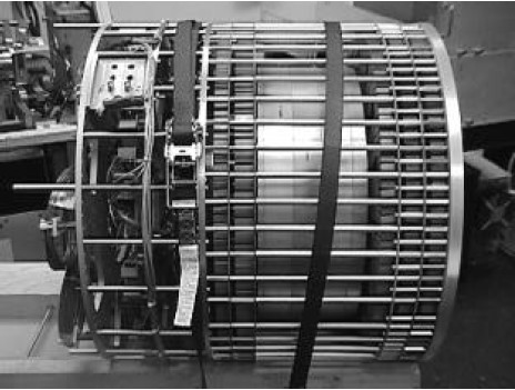
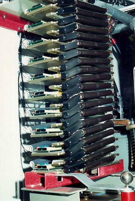
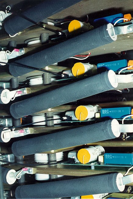
Example Projects:


Solid State Pulsed Power Module (SSPPM) Technical Features

Solid State Pulsed Power Module (SSPPM) Technical Specifications

HV Capacitor Charging Power Supply and SCR Switched SSPPM

HV Capacitor Charging Power Supply and SCR Switched SSPPM Schematic Diagram. A capacitor charging HVPS provides initial charging of the SSPPM. Parallel SCR switches then discharge the pulse energy into a 3 stage magnetic pulse compression circuit and pulse transformer in order to generate the final output pulse delivered to the laser chamber load.

Command Resonant Charging System and IGBT Switched SSPPM

Command Resonant Charging System and IGBT Switched SSPPM Schematic Diagram. A HVPS and command resonant charging system (with de-qing) provide fast pulse charging of the SSPPM for the high (4000 Hz and above) repetition rates necessary for these applications. Dual parallel IGBTs then discharge the pulse energy into a two stage magnetic pulse compressor and pulse transformer.

MOPA SSPPM Electrical Schematic Diagram

MOPA SSPPM Electrical Schematic Diagram shows the HVPS and command resonant charging system (with de-qing circuit) charging up two parallel, identical SSPPM systems (for MO and PA laser channels). The common charging system in this case minimizes timing variation between Master Oscillator and Power Amplifier laser channels due to charging voltage differences which would then translate into timing variation in the magnetic pulse compression stages.

EUV SSPPM Module Hardware

EUV Dense Plasma Focus (DPF) SSPPM Hardware.   From left to right shows the magnetic switch bias circuitry, the series diode and IGBT trigger hardware, the IGBT switches, the C0 capacitor bank, the C1 capacitor bank, the pulse transformer, and the C2 capacitor bank. The DPF load chamber would be attached on the right end of the machine.

More details on the technical design and performance of these particular modulator systems can be found in the published technical papers on the "Decade of Solid State Pulsed Power Module Development at Cymer Inc.", "Solid State Pulsed Power Module (SSPPM) Design for a Dense Plasma Focus (DPF) Device for Semiconductor Lithography Applications" and the "Lifetime and Reliability Data of Commercial Excimer Laser Power Systems Modules" for these modulators.

Back to top


520 MW Klystron Modulator Resonant Charging System Technical Features

  • Application: High power klystron modulator
  • 45 kV, solid state (SCR), Command Charging Switch assembly with fiber optic trigger system initiates resonant charging of modulator PFNs
  • 1 Henry, oil insulated, water cooled, Charging Inductor with secondary, de-qing winding
  • Solid state de-qing switch and circuit allows precise regulation of PFN charging voltage
  • Solid state charging diode assembly
  • De-spiking networks reduce transient voltages on components

520 MW Klystron Modulator Resonant Charging System Technical Specifications

  • Input voltage: Up to 45 kV
  • Output voltage: Up to 75 kV
  • Resonant charging time: 5 ms
  • Continuous Rep-rate: Up to 50 Hz
  • Average power: 380 kW
  • Output regulation: ~+/-0.2%

520 MW Klystron Modulator Floorplan Layout

520 MW Klystron Modulator Resonant Charging 45 kV Solid State Switch Assembly sitting on top of charging inductor housing. Twenty series connected SCRs are clamped in heat sink plates. The right side of the picture shows the grading resistors used to help ensure equal voltage sharing across the series array. To the left of the resistors are break-over diodes incorporated into the fiber-optic coupled trigger circuits to ensure that the devices are quickly turned-on in the case of an overvoltage condition. The fiber optic trigger circuit also derives all its power requirements from the voltage impressed across the switch assembly prior to firing, eliminating the requirement for isolated power specifically used for just the triggering. To reduce the overall volume of the assembly, half the trigger circuits are located on the near side of the switches with the other half on the far side. A number of the trigger fibers can be seen running down the left side of the switch assembly and feeding into the trigger circuits.

520 MW Klystron Modulator Phase Controller, Controls, Charging System

520 MW Klystron Modulator Resonant Charging 45 kV Solid State Switch Assembly Close-Up showing the SCRs in the center left, additional power resistors used in the RC grading network, and four of the trigger circuit boards with fibers feeding into the boards with the trigger signal. Also shown are the insulating threaded rods which run vertically through the switch and clamp the overall assembly together, sandwiching the SCR devices between the heat sink plates.

520 MW Klystron Modulator Controls, Resonant Charging System, and PFN

520MW Klystron Modulator De-Qing Network mounted on the wall of the system enclosure. The de-qing switch is a single SCR mounted between a water cooled heat sink and located in the top right of the de-qing assembly. An array of capacitors sit next to the de-qing switch in order to critically damp the energy remaining in the circuit and dissipate it prior to the next pulse in the de-qing resistor assembly which takes up the bottom majority of the assembly. These 24 hockey puck shaped ceramic resistors are sandwiched between a number of water cooled cold plates. The overall assembly is then clamped together with insulating threaded rod. Finally, underneath the de-qing switch are a set of water manifolds which distribute the cooling water to the overall assembly to each of the water cooled cold plates and components.

520 MW Klystron Modulator PFN Charging Current and Voltage

520 MW Klystron Modulator PFN Charging Current and Voltage Waveforms  shows the half-sinusoidal PFN resonant charging current waveform (terminated somewhat early by the de-qing process) and the typical "1-cos" PFN voltage waveform associated with command resonant charging ending with a voltage of 71.2 kV on the PFN capacitors.

More details on the technical design and performance of this overall modulator system can be found on the Ness Engineering Line Type Modulator Experience page and in the published technical papers on the 520 MW Klystron Modulator System and the Command Resonant Charging System for this modulator.

Back to top


0.5 MW (Avg.) 60 kHz Solid State Modulator Technical Features

  • Customer: Lawrence Livermore National Laboratory
  • Application: Atomic Vapor Laser Isotope Separation (AVLIS) extractor (plate) power supply
  • 6 kV, 80 A dc power supply
    • 12 pulse, 480 V, SCR phase control provides adjustment and regulation
    • Air insulated Transformer/Rectifier (T/R) set
  • 40 (series) x 60 (parallel) MOSFET series switch array generates output pulses into capacitive load
  • 40 (series) x 10 (parallel) MOSFET shunt switch ("tailbiter") array terminates output pulses and discharges capacitive load
  • GTO switched "pre-pulse" generator provides initial "test" pulse
  • Biased saturable reactor limits fault currents until MOSFET arrays have sufficient time to turn off
  • Computer interface, as well as local/remote control panels, allows operation from LLNL computer
  • Diverter system operates in case of a load short circuit fault
    • 2 (redundant) ignitron crowbar switches dissipate energy stored in 570 mF capacitor bank
    • Diverter also protects MOSFET switch arrays

0.5 MW (Avg.) 60 kHz Solid State Modulator Technical Specifications

  • Input voltage: Up to -6 kV
  • Output voltage: -500 to -5500 V
  • Peak current: 700 A
  • RMS current: 150 A
  • Average current: 80 A
  • Current pulse rise time: less than 500 ns
  • Current decay time: 3 ms (e-fold)
  • Pulse on-time: ~16 ms to dc
  • Inter-pulse time: 1.75 ms to 256 ms
  • Rep-rate: dc or 5.5 kHz to 30 kHz (60 kHz at reduced power)
  • Peak power: 4.2 MW
  • Average power: 0.5 MW

60 kHz Modulator Series FET PCB Assembly

60 kHz Modulator Series FET PCB Assembly showing main power board connections to backplane at top. Twenty parallel connected Power MOSFETs are attached to the three water-cooled, cold-plate, heat sink plates running vertically in the photo. The fiber optic trigger receiver and status confirmation transmitter are located in the bottom right side of the picture underneath an aluminum EMI shield. Three sets of additional trigger fan-out drive circuitry are located at the bottom between the heat sinks and the on-board diagnostics circuits located at the bottom edge of the board. Forty of these board assemblies were connected in series in a backplane structure of the modulator to act as the main series switch in providing pulsed energy to the load to charge up the extractor plates.

Close Up View of 60 kHz Modulator Series FET PCB Assembly

Close Up View of 60 kHz Modulator Series FET PCB Assembly showing the details of the MOSFET trigger and voltage protection circuitry. The large resistor is utilized to ensure proper dc voltage grading while transzorb devices ensure similar voltage grading under transient conditions. As can be seen, individual fuses are utilized to isolate each MOSFET cell from the parallel neighbors in the case of a device short circuit fault.

Mounting of Power MOSFETS on 60 kHz Modulator Series FET PCB Assembly

Mounting of Power MOSFETS on 60 kHz Modulator Series FET PCB Assembly is shown in this photo.

60 kHz Modulator Shunt FET PCB Assembly

60 kHz Modulator Shunt FET PCB Assembly  showing the four series connected sections of 10 parallel Power MOSFETs. Since the shunt or "tailbiter" switch in this application required less RMS current capability, only 10 parallel MOSFETs were necessary in each series section. As a result, each similarly sized PCB assembly could contain four series sections and a total of 10 Shunt FET PCB assemblies were required in the modulator for the overall Shunt switch.

Overall 60 kHz Modulator Series FET Assembly

Overall 60 kHz Modulator Series FET Assembly  showing all 40 series-connected Series FET PCB assemblies stacked on edge and installed into the modulator backplane. As can be seen, fiber optic connections are looped down from the top of each board into the transmitter and receiver connections while cooling water inlet and outlet connections are made at the bottom of each PCB assembly.

60 kHz Modulator Overall Enclosures

60 kHz Modulator Overall Enclosures  showing the modulator Transformer/Rectifier (T/R) Set and Phase Controller enclosure on the far right. The near enclosure on the left side contains the dc filter capacitor bank and ignitron diverter switch assembly located in the bottom half of the cabinet (the diverter electronics chassis indicators can be seen in the window of the bottom right). On top of that is the modulator portion of the system. The Series FET assembly is located in the back half of the enclosure (on the far side) while the Shunt FET assembly is lcoated in the middle bay of the top near side. To the left of the Shunt FET assembly are several operator control chassis for local control of the HVDC power supply as well as the modulator.

More details on the technical design and performance of this overall modulator system can be found in the published technical papers on the 0.5 MW 60 kHz Solid State Power Modulator and the High Power Switching Using Power FET Arrays for this modulator.

Back to top


Send consulting inquiries, comments, and suggestions to nessengr@san.rr.com

[BACK] [HOME] [RESUME] [PUBLICATIONS] [NEWS] [LINKS] [CAPABILITIES] [TECHDATA]

Ness Engineering, Inc.
P.O. Box 261501
San Diego, CA 92196
(858) 566-2372
(858) 240-2299 FAX

© Richard M. Ness and Ness Engineering, Inc.
Last Updated:

Website File Auto-Update Javascript courtesy of www.javafile.com   Download the Script